Original Link: https://www.anandtech.com/show/21375/tsmc-readies-8x-reticle-size-super-carrier-interposer
TSMC Readies 8x Reticle Super Carrier Interposer For Next-Gen Chips Twice as Large As Today's
by Anton Shilov on April 30, 2024 9:00 AM ESTTSMC is no stranger to building big chips. Besides the ~800mm2 reticle limit of their normal logic processes, the company already produces even larger chips by fitting multiple dies on to a single silicon interposer, using their chip-on-wafer-on-substrate (CoWoS) technology. But even with current-gen CoWoS allowing for interposers up to 3.3x TSMC's reticle limit, TSMC plans to build bigger still in response to projected demand from the HPC and AI industries. To that end, as part of the company's North American Technology Symposium last week, TSMC announced that they are developing the means of building super-sized interposers that can reach over 8x the reticle limit.
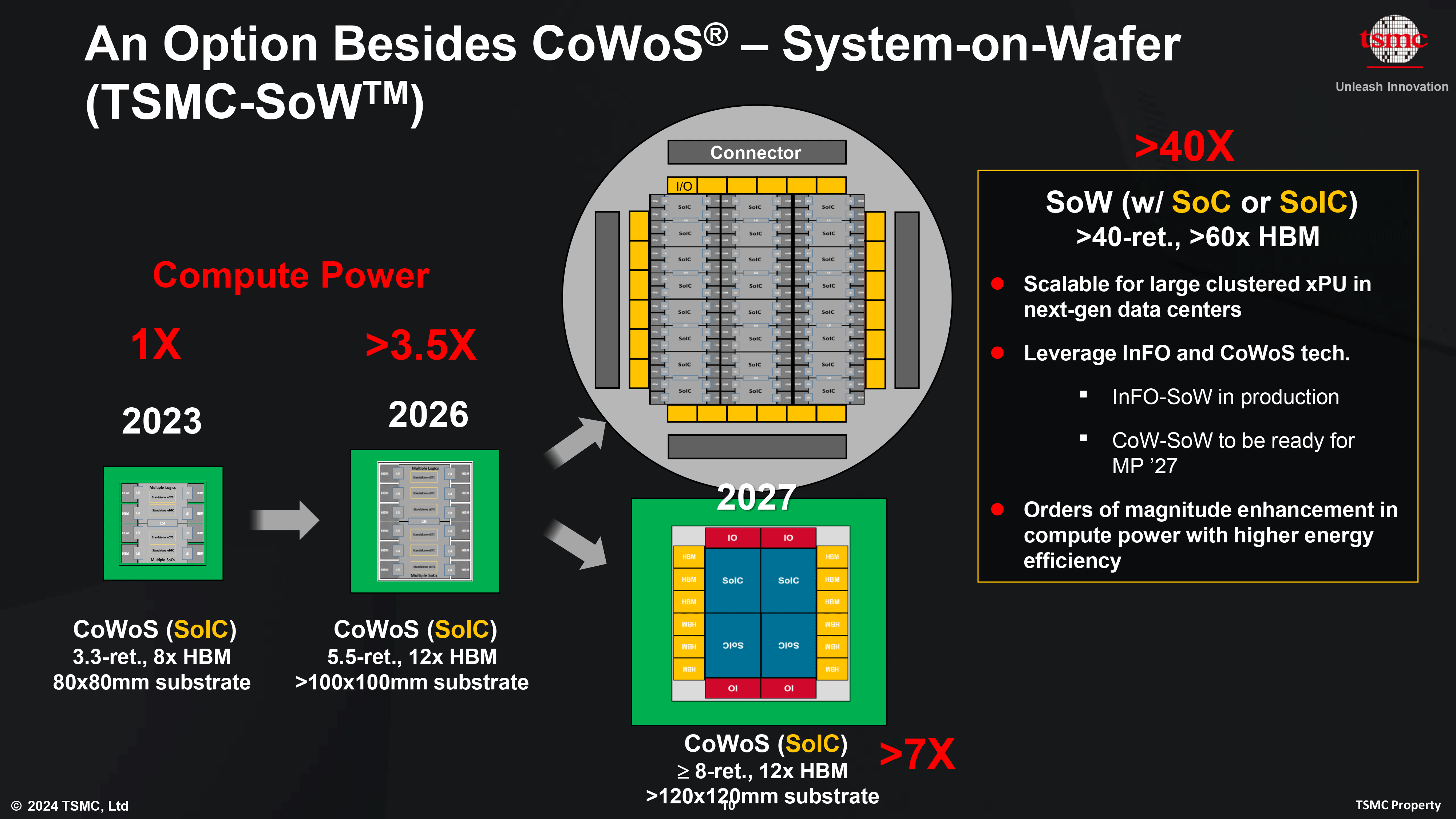
TSMC's current-generation CoWoS technology allows for building interposers up to 2831 mm2 and the company is already seeing customers come in with designs that run up to those limits. Both AMD's Instinct MI300X accelerator and NVIDIA's forthcoming B200 accelerator are prime examples of this, as they pack huge logic chiplets (3D stacked in case of AMD's product) and eight HBM3/HBM3E memory stacks in total. The total space afforded by the interposer gives these processors formidable performance, but chip developers want to go more powerful still. And to get there as quickly as possible, they'll need to go bigger as well in order to incorporate more logic chiplets and more memory stacks.
For their next-generation CoWoS product that's set to launch in 2026, TSMC plans to release CoWoS_L, which will offer a maximum interposer size of approximately 5.5 times that of a photomask, totaling 4719 mm² altogether. This next generation package will support up to 12 HBM memory stacks and will necessitate a larger substrate measuring at 100×100 mm. Coupled with process node improvements over the next few years, and TSMC expects chips based on this generation of CoWoS to offer better than 3.5x the compute performance of current-generation CoWoS chips.
Farther down the line, in 2027 TSMC intends introduce a version of CoWoS that allows for interposers up to 8 times larger than the reticle limit. This will offer an ample 6,864 mm² of space for chiplets on a substrate that measures 120×120 mm. TSMC envisions leveraging this technology for designs that integrate four stacked systems-on-integrated chips (SoICs), with 12 HBM4 memory stacks and extra I/O dies. TSMC roughly projects that this will enable chip designers to once again double performance, producing chips that surpass 7x the performance of current-generation chips.
Of course, building such large chips will come with its own set of consequences, above and beyond what TSMC will have to deal with. Enabling chip designers to build such grand processors is going to impact system design, as well as how datacenters accommodate these systems. TSMC's 100×100mm substrate will be riding right up to the limit of the OAM 2.0 form factor, whose modules measure 102×165mm to begin with. And if that generation of CoWoS doesn't break the current OAM form factor, then 120×120mm chips certainly will. And, of course, all of that extra silicon requires additional power and cooling, which is why we're already seeing hardware vendors prepare for how to cool multi-kilowatt chips by investigating liquid and immersion cooling.
Ultimately, even if Moore's Law has slowed to a crawl in terms of delivering transistor density improvements, CoWoS offers an out for producing chips with an ever-larger number of transistors. So with TSMC set to offer interposers and substrates with over twice the area of today's solutions, big chips intended for HPC systems are only going to continue to grow in both performance and size.
Related Reading
- TSMC's 1.6nm Technology Announced for Late 2026: A16 with "Super Power Rail" Backside Power
- TSMC 2nm Update: N2 In 2025, N2P Loses Backside Power, and NanoFlex Brings Optimal Cells
- TSMC Preps Cheaper 4nm N4C Process For 2025, Aiming For 8.5% Cost Reduction
- TSMC's System-on-Wafer Platform Goes 3D: CoW-SoW Stacks Up the Chips
- TSMC Jumps Into Silicon Photonics, Lays Out Roadmap For 12.8 Tbps COUPE On-Package Interconnect


